Tag: electronics
Main Attraction: Scientists Create World’s Thinnest Magnet

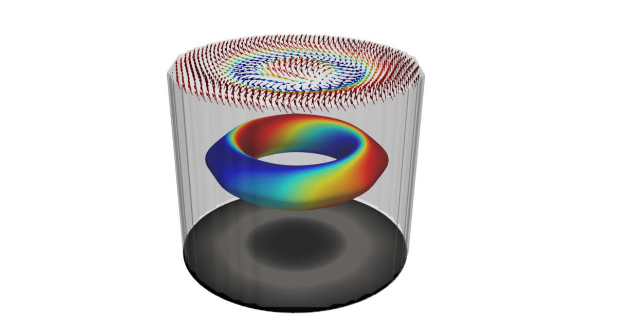
The Spintronics Technology Revolution Could Be Just a Hopfion Away
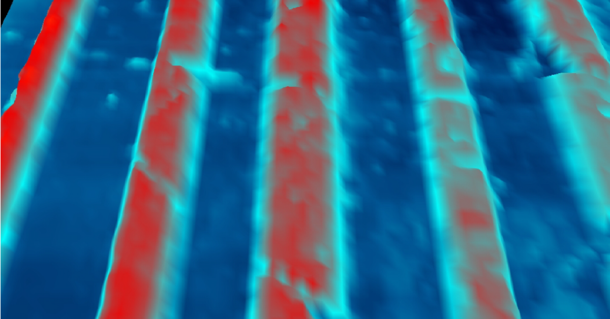
An Innovative Pattern: Scientists Rewrite Rules for 2D Electronics
2D Electronics Get an Atomic Tuneup
Toward an Ultrahigh Energy Density Capacitor
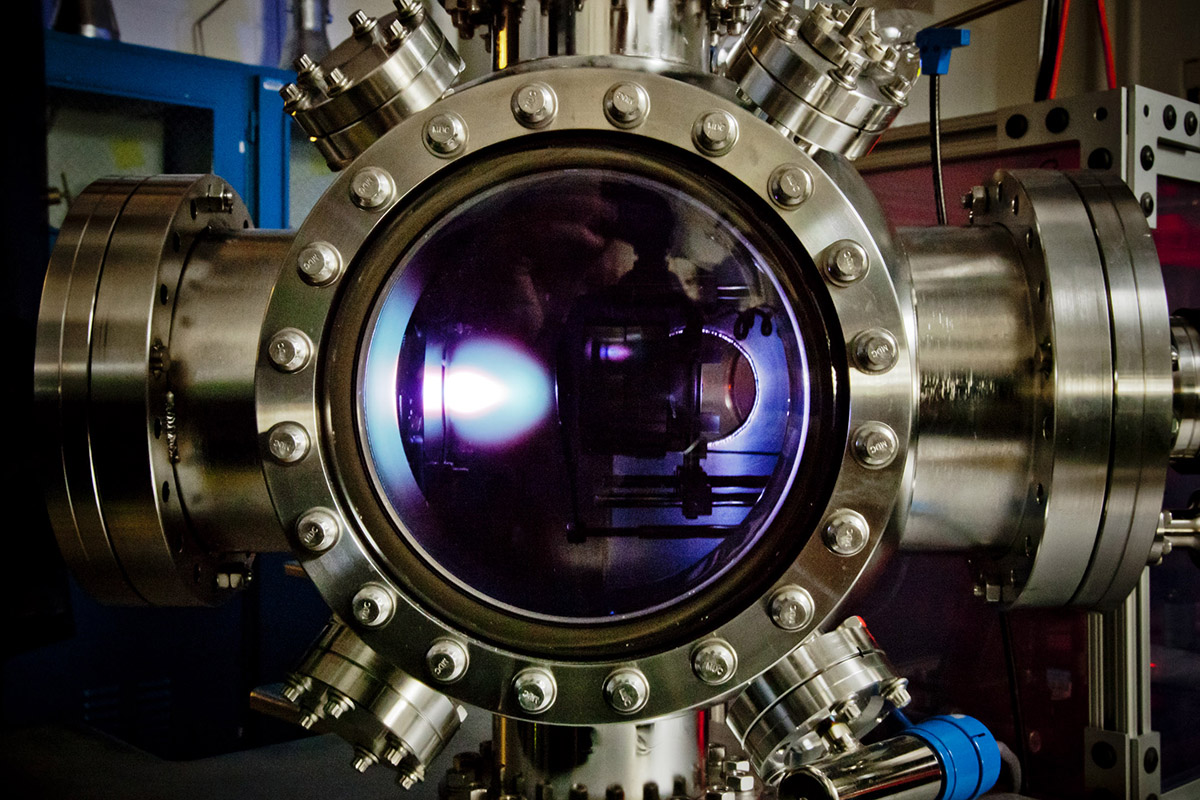
The Best Topological Conductor Yet: Spiraling Crystal Is the Key to Exotic Discovery
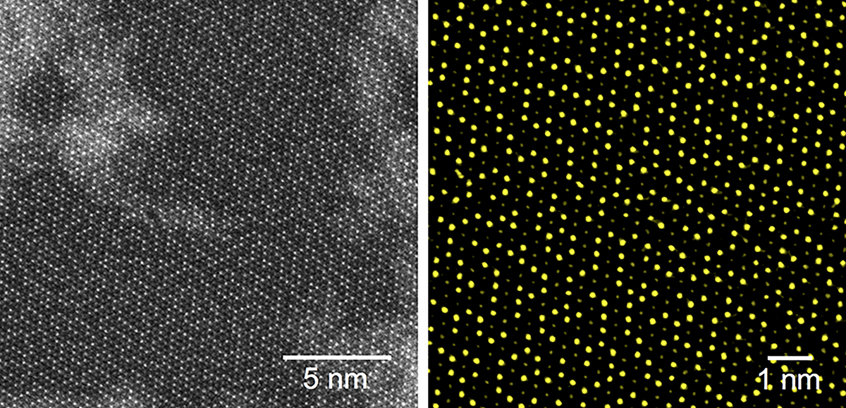
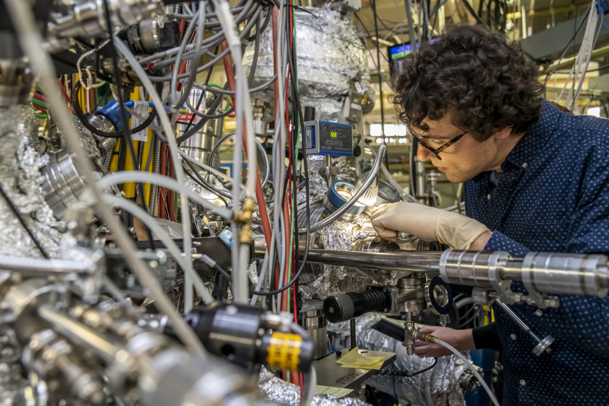
Scientists Take a Deep Dive Into the Imperfect World of 2D Materials
Topological Matters: Toward a New Kind of Transistor
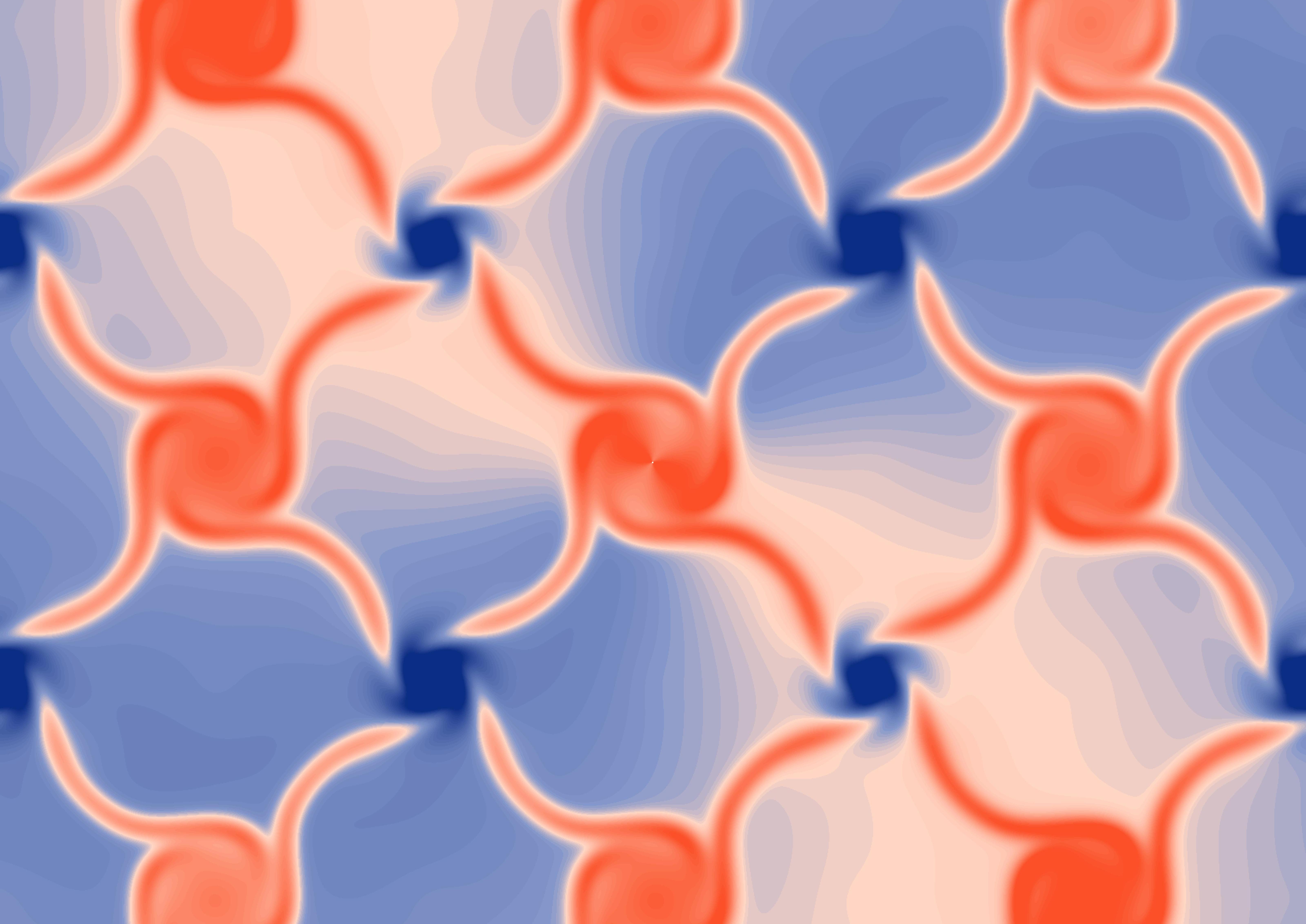
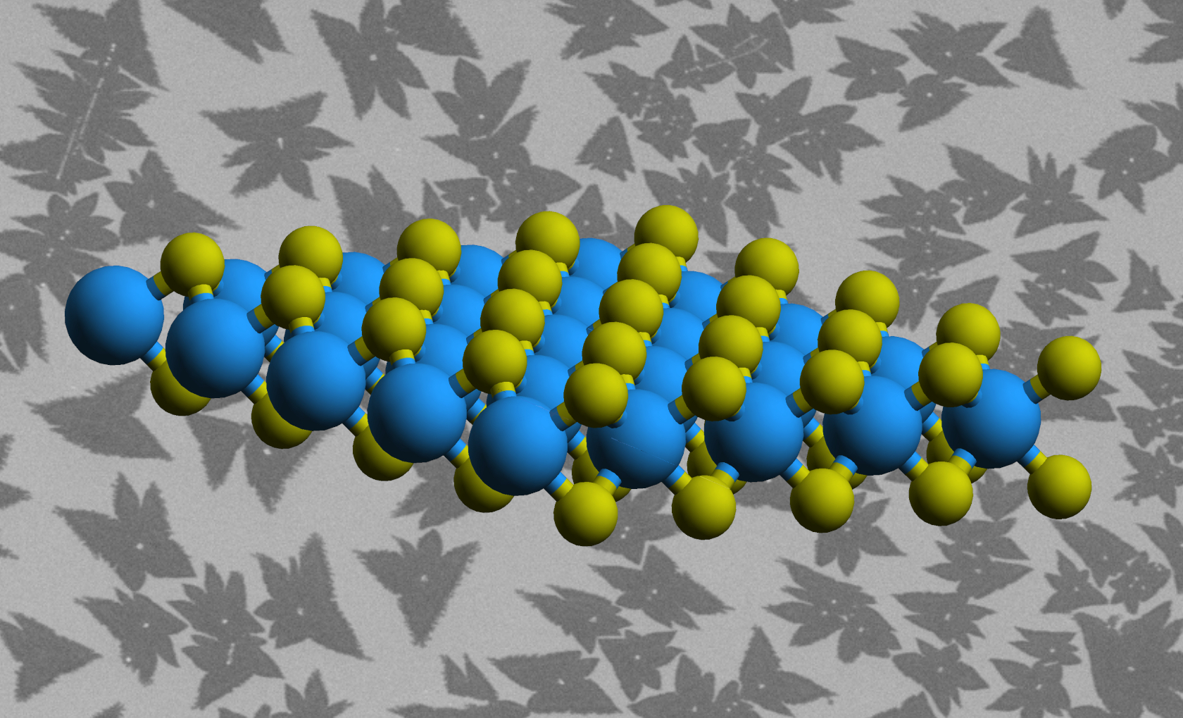
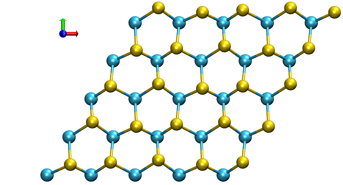
Scientists Discover ‘Chiral Phonons’ – Atomic Rotations in a 2-D Semiconductor Crystal
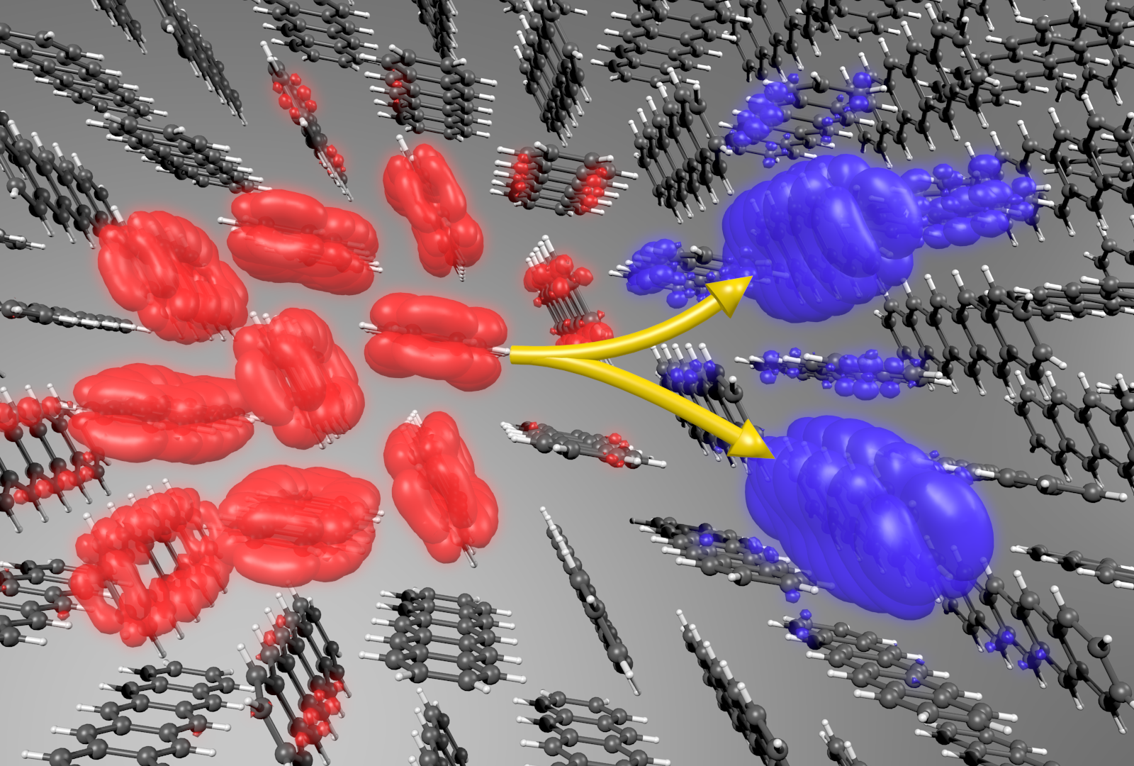
New Discovery Could Improve Organic Solar Cell Performance
A New Spin on Quantum Computing: Scientists Train Electrons with Microwaves
Simplifying Solar Cells with a New Mix of Materials