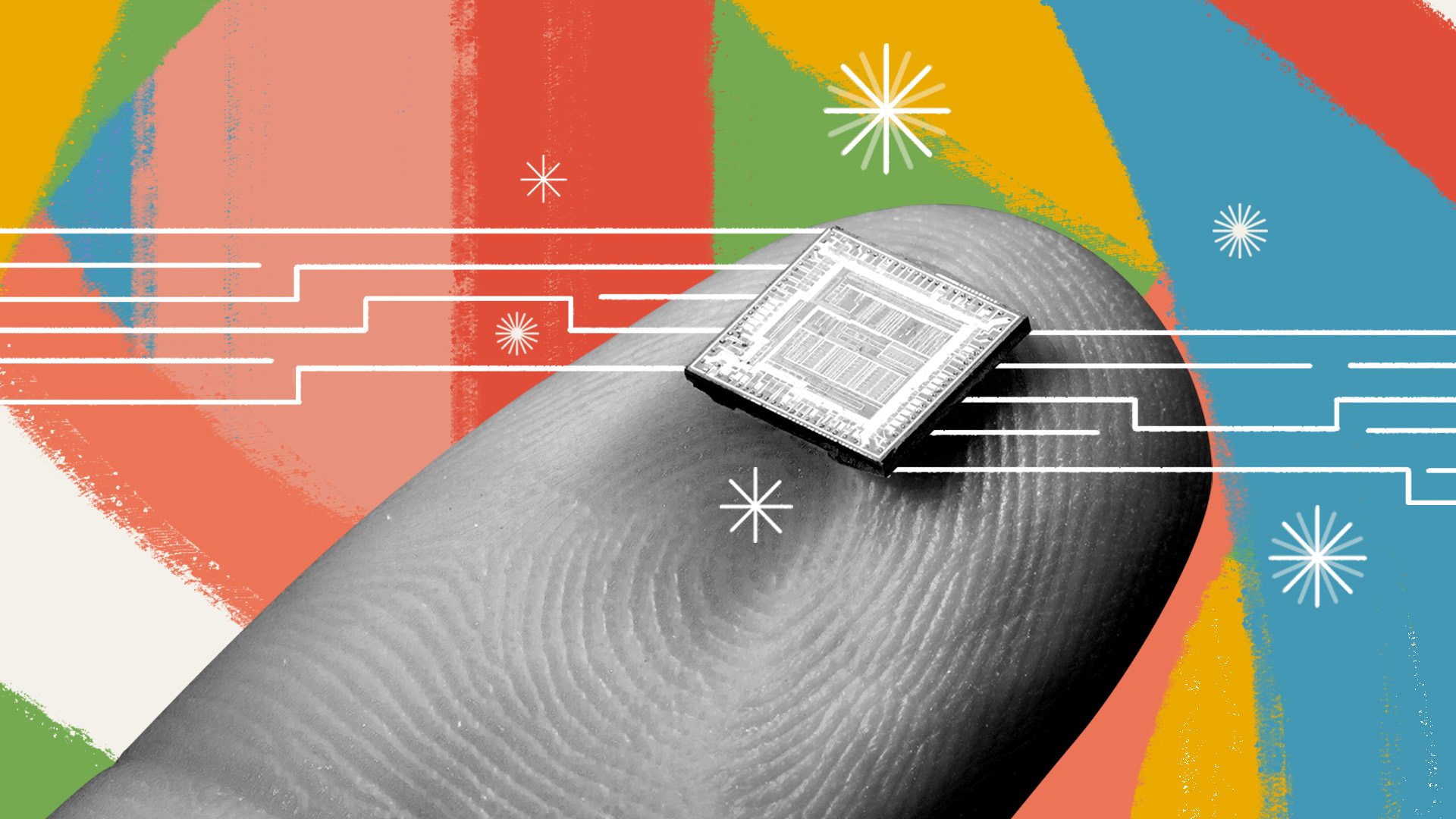
A new center led by Lawrence Berkeley National Laboratory (Berkeley Lab) could accelerate the next revolution in microchips, the tiny silicon components used in everything from smartphones to smart speakers, life-saving medical devices, and electric cars.
The new center, called CHiPPS – or the Center for High Precision Patterning Science – is led by Berkeley Lab microelectronics expert Ricardo Ruiz. He is also a staff scientist in Berkeley Lab’s nanoscience user facility, the Molecular Foundry.
“Advanced computer chips are essential to modern life. Staying at the forefront of this technology – and keeping pace with Moore’s Law – is critical to our economic security and national defense,” Ruiz said.
Over the course of four years, Ruiz and his research partners will direct their diverse scientific expertise toward a common goal: Gaining new insight into the science of extreme ultraviolet lithography or EUVL, a revolutionary technique that enables the world’s leading semiconducting manufacturers to pack more than 100 billion transistors – the tiny components that help a computer retain and process data – into a chip the size of a fingernail.
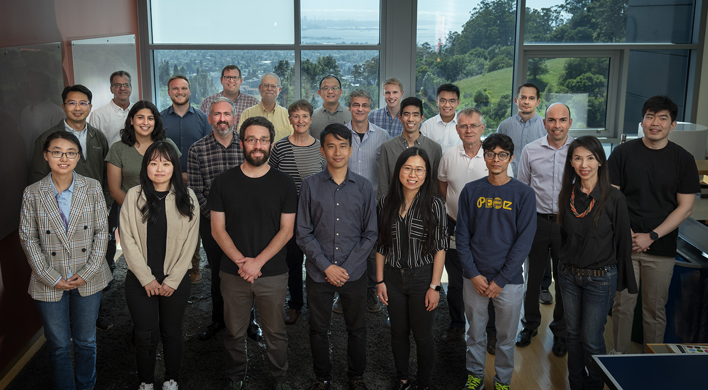
The team includes Berkeley Lab scientists from the Molecular Foundry, the Advanced Light Source, the Center for X-Ray Optics, the Chemical Sciences Division, and the Energy Storage & Distributed Resources Division, along with collaborators from Argonne National Laboratory, San José State University, Stanford University, the University of California at Santa Barbara, and Cornell University.
The researchers’ work could help chip manufacturers make even smaller, more powerful chips, and support the goals of the Creating Helpful Incentives to Produce Semiconductors and Science Act, which aims to mitigate supply chain disruptions by helping the U.S. design and produce the world’s most advanced chips domestically. (The CHIPS and Science Act was signed into law by President Joe Biden last summer.)
“Advanced computer chips are essential to modern life. Staying at the forefront of this technology – and keeping pace with Moore’s Law – is critical to our economic security and national defense.”
– Ricardo Ruiz, Berkeley Lab CHiPPS Director
Last year, the U.S. Department of Energy awarded the CHiPPS research center a total of $11.5 million over four years through the Energy Frontier Research Centers program to pursue fundamental research in EUV lithography, including new materials and their interaction with EUV light. The CHiPPS center’s efforts comprise four research “thrusts” focused on photomaterials synthesis, new “hierarchical” self-assembling materials, theory and modeling, and new techniques to characterize EUV lithography materials with atomic precision.
The CHiPPS research center not only aims to advance EUVL research, but it also places great emphasis on workforce development to nurture the next generation of scientists and engineers, Ruiz said. Through a collaboration with San José State University, the CHiPPS center offers an immersive work training program to four students every summer, consisting of two undergraduate students and two master’s students. (The inaugural cohort commenced in June.)

Ricardo Ruiz
Before joining Berkeley Lab in 2019, Ruiz worked as a research scientist in the microelectronics and data storage industry, specializing in polymer-based lithography techniques for magnetic data storage at Hitachi Global Storage Technologies, and alternative nanofabrication techniques for non-volatile memories at Western Digital. He earned his Ph.D. in physics from Vanderbilt University in 2003, and worked as a postdoctoral researcher at Cornell and IBM before joining Hitachi Global Storage Technologies in 2006.
He shares his perspective in this Q&A.
Q. How will the new CHiPPS Energy Frontier Research Center advance microelectronics?
Ricardo Ruiz: The mission of the CHiPPS center is to create new fundamental understanding and control of patterning materials and processes with atomic precision. The goal is to enable the large-scale manufacturing of next-generation microelectronics.
To unpack that a little bit, that means that our focus lies in the scientific exploration of an advanced method known as extreme ultraviolet (EUV) lithography.
EUV lithography is key to creating integrated-circuit patterns on the scale of a billionth of a meter in the materials that are used to manufacture advanced microchips. It’s the latest advance in lithography, a technique that uses light to print tiny patterns in silicon to mass produce microchips.
Over the past five decades, lithographic techniques have progressively evolved from the use of light in the visible range, where wavelengths are as small as 400 nanometers, to the latest advance: the extreme ultraviolet range with short wavelengths of 13.5 nanometers, about 40 times smaller than the wavelengths of visible light. Such advances in lithography have enabled the use of smaller and smaller wavelengths to fabricate smaller, denser microchips.
EUV lithography was just recently introduced in the production of microchips in 2019, and it still faces multiple challenges, particularly in the development of advanced patterning materials suitable for high-resolution and high-throughput manufacturing processes using light in the form of EUV radiation.
The light-sensitive chemical films called photoresists or “resists” in use today for microchip production do not efficiently absorb EUV radiation, and little is known about how these photoresists interact with EUV light.
And that’s where we come in.
At CHiPPS, we are taking this opportunity to design new photoresist materials specifically designed to work with EUV radiation. We aim to tackle fundamental scientific challenges to better understand and control the chemical reactions arising from the interaction between EUV radiation and resist materials. These tiny, but localized, chemical changes inside the resist is what enables the fabrication of smaller patterns to print, for example, smaller transistors, facilitating the production of faster and denser microchips.
Q. The microelectronics industry already has a wealth of 50 years of experience in lithography. How is the CHiPPS EFRC’s approach to lithography different?
Ruiz: EUV radiation is fundamentally a very different light from the previous generations of light that the chip industry had used for the past 50 years.
And it wasn’t too long ago when the chip industry used deep ultraviolet light (193 nanometers) to print transistor patterns on silicon, a key component in chip production.
EUV lithography uses a wavelength of light that is only 13.5 nanometers. That’s a factor of 10 smaller than the previous generation, which makes EUV photons 10 times more energetic.
Unfortunately, conventional deep UV photoresists are very poor absorbers at EUV wavelengths. Furthermore, when EUV light does get absorbed, its high-energy photons kick electrons off the resist and substrate materials. This in turn pushes other “secondary” electrons around in a cascading event.
And that is the issue with the photoresist materials in use today: It is the secondary low-energy electrons that are making chemical changes in the photoresist. This is poorly understood and poorly controlled, because there is very little knowledge of how materials behave at the atomic level when they interact with EUV light.
This is a challenging problem to solve, but fortunately we have the strength of having a big interdisciplinary team. We paid special attention in selecting the brightest minds in all aspects of patterning science with a proven record of collaboration and team science.
Our interdisciplinary team of 13 principal investigators span the scientific disciplines, from synthetic chemistry to nanomaterials and physics to computer modeling. Our scientists come from some of the nation’s leading national labs and universities, including Berkeley Lab, Stanford University, San José State University, UC Santa Barbara, Argonne National Laboratory, and Cornell University.
Everyone in the team is very excited to work together. We’re exploring new physics and new chemistry, and we all have the same goal: Pushing the boundaries of patterning materials so we can help the microchip industry stay ahead of Moore’s Law. (Moore’s Law is named after Intel co-founder Gordon Moore, who declared in 1965 that the number of transistors placed on a chip would double every two years until the technology reached its limitations in miniaturization and performance.)
Q. How are CHiPPS and Berkeley Lab uniquely positioned to advance EUV lithography with the microchip industry?
Ruiz: As a multidisciplinary national lab, Berkeley Lab offers a combination of research facilities; access to big, scientific instruments; and expertise in chemistry, materials science, physics, engineering, and computing – and proximity to industry and universities – that can’t be found anywhere else.
Berkeley Lab is also home to the Center for X-Ray Optics and the Advanced Light Source.
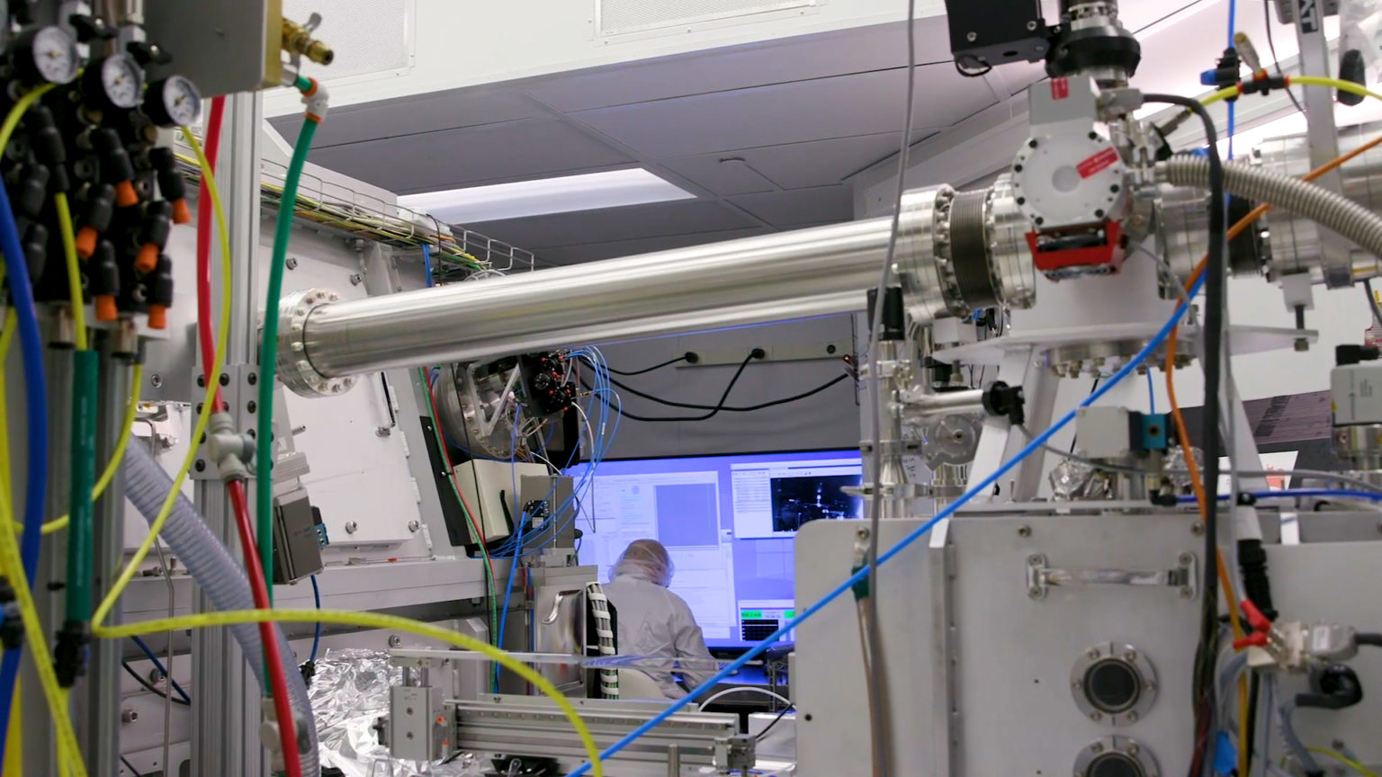
The Advanced Light Source (or ALS) is a synchrotron user facility that produces very bright X-rays, including soft X-ray and extreme ultraviolet light, that are critical to characterizing photoresist materials.
In very close proximity to the ALS is the Center for X-Ray Optics (or CXRO), which is dedicated to advancing science and technology by using short wavelength optical systems and techniques with a special emphasis on EUV technology.
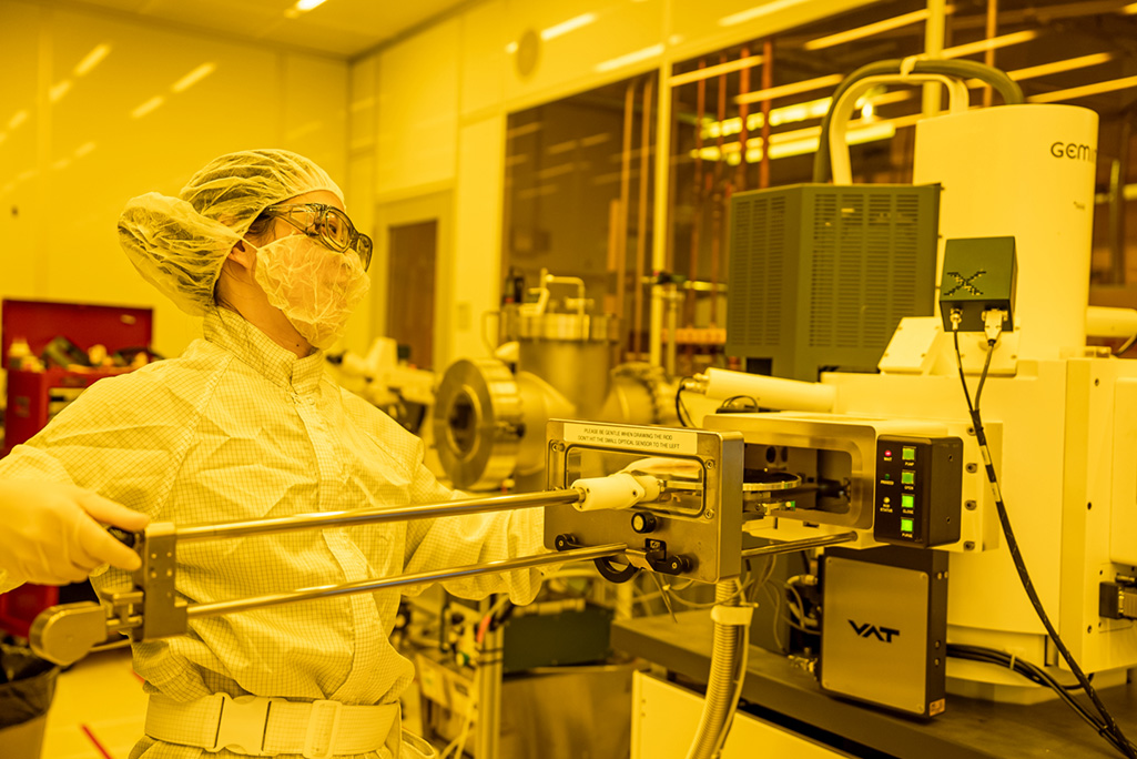
CXRO houses a unique lithography platform called a “high numerical aperture EUV exposure tool,” which offers a resolution capability that is significantly better than current state-of-the-art EUV platforms. CXRO is currently the only research facility in the world where industry partners can use this tool to test new patterning materials.
There are only a few places in the world where people can do research with EUV light because it’s very expensive and very difficult to make EUV light and EUV optics. For example, a first-generation EUV lithography tool costs more than $100 million. That’s not something that research labs or even microchip industries can afford to buy just for research.
CXRO is strategically positioned to help chip manufacturers like Intel and Samsung do EUV lithography research without having to buy a $100 million EUV lithography tool. Additionally, CXRO, along with its close neighbor the ALS, offers unique capabilities and scientific expertise that are critical in understanding how EUV light interacts with photoresist materials.
But microchip patterning science requires much more than EUV exposure and characterization capabilities. We also need specialized instruments and world-class experts in materials synthesis. To that end, we will heavily rely on Berkeley Lab’s Molecular Foundry. Its Organic and Biological Nanostructure facilities are instrumental to making new nanostructured patterning materials that are more sensitive to EUV light.
The Molecular Foundry is also home to a 4,850 square foot clean-room facility dedicated to patterning, nanofabrication, and molecular self-assembly. This facility is critical to developing atomically precise pattern-transfer techniques for new EUV materials.
In our pursuit of a comprehensive understanding of all chemical and physical phenomena, modeling and simulation research around EUV patterning is key. This work is supported by the computational capabilities and expertise at Berkeley Lab’s Chemical Sciences and Energy Storage & Distributed Resources divisions together with computing resources at the Department of Energy’s National Energy Research Scientific Computing Center (NERSC), which is also located at Berkeley Lab.
Q: Pushing the boundaries of Moore’s Law was once considered unthinkable. How does the CHiPPS team aim to advance EUV lithography research in order to stay ahead of Moore’s Law?
Ruiz: Developing high-performance materials capable of high EUV light absorption and precise lithography patterns formed through controlled, atomic-level chemical reactions are two goals that are crucial to our successfully advancing the limits of Moore’s Law.
To achieve these goals, our CHiPPS researchers are making sure that we take advantage of working together in a team that is larger than the sum of its parts.
Brett Helms (Berkeley Lab), Chris Ober (Cornell), Rachel Segalman (UC Santa Barbara), and Stacey Bent (Stanford) are developing new photoresist materials that are specifically tuned to work with EUV radiation. In a multi-prong collaboration across institutions, Brett leads efforts on a new class of materials called organo-metal halides. Chris and Rachel are advancing bio-mimetic, sequence-specific polymers. And Stacey is pursuing “dry” resists synthesized from layered organometallic materials.
At CHiPPS, we are also exploring “bottom-up” hierarchical materials and processes as a potential solution to overcome the limitations of photoresist materials. For example, Argonne’s Paul Nealey is focused on developing highly customizable block copolymer materials for lithographic features as small as 4 nanometers. (To put that in perspective, a sheet of paper is about 100,000 nanometers thick.) Paul, Stacey, and I are collaborating to employ various self-assembly and pattern transfer methods.
Our teams are also collaborating to understand the thermodynamics of self-assembling polymers on “noisy” or defective EUV patterns. Additionally, we are working with Paul Nealey and CXRO Director Patrick Naulleau to identify and minimize defects in photoresist patterns. A joint effort – led by Stacey Bent’s group at Stanford with my group at Berkeley Lab and Paul Nealey’s group at Argonne – focuses on an area-selective deposition process that precisely transfers circuit patterns from the photoresist to the silicon wafer.
At CHiPPS, computer modeling and simulations are cornerstones to understanding the chemical and physical phenomena behind pattern formation with EUV radiation. Sam Blau and Frances Houle of Berkeley Lab are leading computer modeling and simulation experiments that aim to understand how patterning materials react to EUV light and low-energy electrons. Their work will also help us better understand the chemical and physical processes that take place after light exposure.
They are collaborating closely with Cheng Wang, Oleg Kostko, and Patrick Naulleau of Berkeley Lab and Dahyun Oh of San José State University to use relevant experimental data in their modeling. The team will also provide input to the synthesis efforts of Brett Helms, Chris Ober, Rachel Segalman, and Stacey Bent.
To effectively monitor and validate our materials and processes, CHiPPS will rely on a comprehensive characterization suite developed by Cheng Wang, Oleg Kostko, Patrick Naulleau, Weilun Chau (also of Berkeley Lab), and Dahyun Oh. This suite allows us to image buried features in resist materials, assess the impact of EUV exposure, study secondary electron behavior, measure interface roughness, and understand the role of interfaces in the patterning process.
As you can see, our highly integrated, collaborative team is our greatest asset. We are all motivated by the exciting developments of patterning science. And we are well aware that the challenges in front of us can only be overcome by team science.
The Advanced Light Source, Molecular Foundry, and NERSC are DOE Office of Science user facilities at Berkeley Lab.
How Mentoring Can Advance the Next Generation of Scientists and Engineers
If you ask CHiPPS Director Ricardo Ruiz, mentoring the next generation of scientists and engineers is just as important if not more so than advancing EUV lithography research for next-generation microelectronics. And that comes from someone who knows firsthand how mentoring can inspire and transform a budding interest in STEM (science, technology, engineering, and mathematics) into a flourishing and rewarding career.
“Since joining Berkeley Lab, I’ve been mentoring a good number of student interns in addition to the postdocs in my group. Mentorship has always been important to me. Over the years I’ve been lucky to work with inspiring mentors who shaped my career and now I try, as best as I can, to offer a similar experience to the next generation of scientists who bring a fresh perspective and energy for driving scientific progress. Working with them at Berkeley Lab has been a rewarding and fulfilling experience. Mentorship is a responsibility I take seriously, as it promotes a virtuous cycle of collaboration and knowledge while shaping future leaders in science,” he said.
Below is an excerpt of our discussion with Ruiz on the importance of mentoring in STEM.
Q: You have a Ph.D. in physics, and you’re a leading expert in nanopatterning for microelectronics. Is microelectronics research something you dreamed of pursuing when you were growing up?
Ruiz: Not at all. When I was in high school, I thought I wanted to be an astronomer, but it was later during college and graduate school when I discovered my passion for physics, materials science, and soft matter through a project on organic electronic materials. These are an exciting class of electronic materials that can be deposited onto flexible or soft substrates, enabling flexible electronics and wearable technologies.
After I completed my Ph.D. at Vanderbilt, I continued to specialize in organic electronic materials as a postdoctoral scholar at Cornell University. After that I spent 15 years in the private sector at IBM Research, Hitachi Global Storage Technologies, and most recently at Western Digital where I did research on various nanofabrication and self-assembling techniques for semiconductor, magnetic storage, and memory technologies until I joined Berkeley Lab at the end of 2019. As I look back, it is easy to recognize that much of my career trajectory was shaped by influential and thoughtful mentors along the way who helped me build a career and get to where I am today.
Mentors can make the biggest impact in motivating people to stay in STEM careers and do good quality science that matters not only for personal gain but for the good of society. I was very lucky. I benefited from having excellent mentors who served as role models for me throughout my career.
At CHiPPS, we all value the importance of mentorship, and that’s why we pay special attention to creating opportunities and equitable experiences for the postdocs and students working at the center. We are also excited about the student training program we launched together with San José State University. Through this program, four students have the opportunity to learn and interact alongside Berkeley Lab scientists during the summer.
Q: How does your experience in the private sector shape your approach to scientific research and leadership at Berkeley Lab?
Ruiz: My experience in the private sector has turned out to be a nice complement to my work at Berkeley Lab.
In the private sector, researchers are very focused on applications. And in my work at Berkeley Lab’s Molecular Foundry, we are always trying to look for ways in which science can advance an application, even if it’s fundamental science.
Another experience that shaped my career considerably in the private sector was the focus on team effort. Berkeley Lab is the birthplace of multidisciplinary team science, so it’s a perfect fit.
###
Founded in 1931 on the belief that the biggest scientific challenges are best addressed by teams, Lawrence Berkeley National Laboratory and its scientists have been recognized with 16 Nobel Prizes. Today, Berkeley Lab researchers develop sustainable energy and environmental solutions, create useful new materials, advance the frontiers of computing, and probe the mysteries of life, matter, and the universe. Scientists worldwide rely on the Lab’s facilities for their discovery science. Berkeley Lab is a multiprogram national laboratory managed by the University of California for the U.S. Department of Energy’s Office of Science.
DOE’s Office of Science is the single largest supporter of basic research in the physical sciences in the United States and is working to address some of the most pressing challenges of our time. For more information, please visit energy.gov/science.

Science in Motion: Nano-Materials to Make Better Light Sensors
Pushing the Boundaries of Moore’s Law: How Can Extreme UV Light Produce Tiny Microchips?