Key Takeaways
- Materials known as perovskites show great promise to reduce the costs of solar power but are not yet durable enough to be commercially viable.
- Scientists developed a simplified process to fabricate perovskite solar cell materials with improved durability and efficiency.
- Berkeley Lab researchers used simultaneous characterization techniques to understand why the process worked so well, providing key insights to nudge perovskites closer to commercialization.
For Michael Saliba and Mahdi Malekshahi, it was one of those moments in science when good experimental results raise more questions. The University of Stuttgart researchers recently developed a new process to make solar cells with perovskites – advanced crystalline materials with potential to revolutionize solar technology. Their cells were very efficient and stable, but there was one catch: they did not have a detailed understanding of why this process worked so well.
Saliba and Malekshahi reached out to researchers at the Molecular Foundry, a Department of Energy Office of Science user facility located at Lawrence Berkeley National Laboratory (Berkeley Lab). Fast forward several months, and the Berkeley Lab team has applied a set of techniques to reveal changes in the crystalline structures of perovskite solar cell materials in real time as they were being fabricated with Saliba’s process. The results, published in a recent Advanced Materials paper, provide researchers with a deeper understanding of how to make better perovskite solar cells.
“Material fabrication is often a black box,” said Carolin Sutter-Fella, a Molecular Foundry staff scientist and one of the paper’s corresponding authors. “You can’t see what is happening as the material transforms from its initial building blocks to the final state. We built several capabilities that allow us to watch the formation of perovskite and other printable solar cell materials in fine detail. The insights from this work can help researchers address key barriers to commercializing this promising technology.”
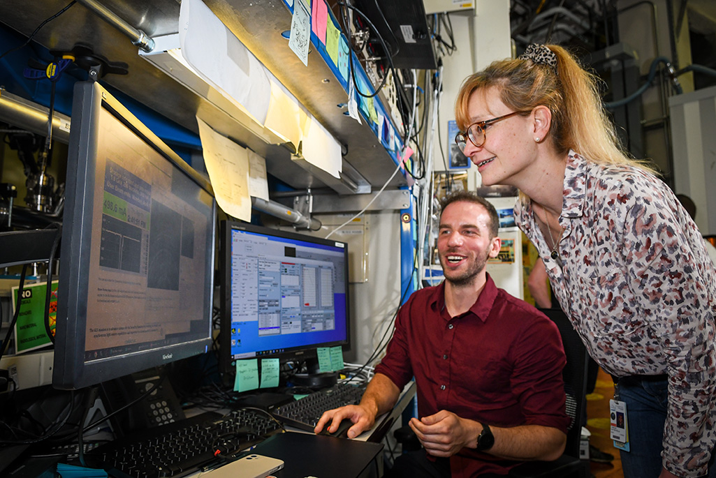
“By continuously taking measurements while depositing the material, we can visually follow how its functional properties evolve,” said Tim Kodalle, a Berkeley Lab postdoctoral researcher at the Molecular Foundry and the study’s lead author. “It’s like watching a video.”
“We built several capabilities that allow us to watch the formation of perovskite and other printable solar cell materials in fine detail. The insights from this work can help researchers address key barriers to commercializing this promising technology.”
– Carolin Sutter-Fella
The work was also conducted at the Advanced Light Source, a Department of Energy Office of Science User Facility located at Berkeley Lab.
A potential game-changer for solar
Perovskites have numerous advantages over the traditional silicon-based solar panels that dominate the solar industry today. For one, they absorb light much more efficiently. As a result, they can be made 100 times thinner and even printed on surfaces. Because they require less material and lower temperatures to process, they are potentially less expensive to produce. Unlike silicon or other semiconductor panels, perovskites perform well with material impurities.
The elemental composition of perovskites can easily be changed so that they absorb different parts of the sun’s spectrum, which opens exciting opportunities to apply thin perovskite films to silicon panels. The resulting “tandem” panels could be significantly more efficient than today’s panels, potentially enabling cost savings to accelerate the clean energy transition.
Despite these advantages, perovskite solar panels are not commercially viable yet. The main barrier is a lack of stability and durability. Solar panels must be able to last for 20 to 30 years in all kinds of weather. Perovskites attract water and degrade quickly in humid conditions, limiting their long-term durability in the field. Because of their sensitivity to environmental conditions, it’s also difficult to fabricate perovskite cells with consistent quality.
“Two different labs may use the same process to make perovskites with significantly different quality,” said Sutter-Fella. “This makes it hard for researchers to reproduce experiments, compare results, and figure out why some solar cells perform better than others.”
A protective barrier to keep out moisture
One approach to improve durability involves fabricating a perovskite solar cell and then depositing an organic molecule called phenethylammonium chloride or PEACl on its surface. Researchers studying this two-step process have found that the PEACl forms a thin protective barrier that is effective at keeping out moisture.
Saliba’s team at the University of Stuttgart improved this process by integrating perovskite cell fabrication and PEACl deposition into a single step. “Such a simplified process can enable researchers to make cells with more consistent quality,” said Kodalle. “Longer term, the process can potentially reduce the costs and energy consumption of perovskite cell manufacturing.”
Saliba’s lab found that cells made with his process were more durable and efficient than cells made without PEACl. The collaboration with Berkeley Lab provided a more detailed explanation of this observation, characterizing how the perovskite materials evolved structurally as they were made.
Probing perovskites with X-rays, laser beams, and white light
In an approach known as multimodal imaging, the Berkeley Lab team applied three techniques to probe perovskite solar cell materials during fabrication, observing the evolution of their properties as they formed. Two materials were evaluated – one treated with PEACl using the process from Saliba’s lab and the other without PEACl. The results revealed critical differences in the evolution of the two samples.
The first technique, known as grazing incidence wide-angle X-ray scattering, was conducted at the Advanced Light Source, a circular particle accelerator that generates bright X-ray beams. The technique involved illuminating the samples with a beam of X-rays at a shallow angle and measuring the resulting pattern of the X-rays as they scatter off of the atoms in the sample. This information revealed changes in the crystalline structures during the formation of the perovskite layers.
The second technique, called photoluminescence spectroscopy, measured the light emitted by the samples when illuminated by a laser. The changes in the energy of the light emitted by the samples provided insight into their crystal quality. A third technique, conducted at the Molecular Foundry, involved shining white light on the samples and determining the portion of light absorbed by the samples. This technique revealed complementary information to the photoluminescence spectra and X-ray scattering patterns, providing additional insights into the crystal structure of the samples. The researchers then correlated the data streams from the three techniques to produce a detailed understanding of the temporal evolution of the crystalline structure of the samples.
The techniques revealed that the crystals in the PEACl-treated samples grew more slowly and were of higher quality, with a protective PEACl-rich layer forming at their surface. The team believes these findings explain the cells’ improved efficiency and stable operation for over a month.
Sutter-Fella envisions several possible next research steps. “We can treat perovskites with other molecules and see how they affect durability and efficiency,” she said. “We also need to monitor the cell’s stability over a longer period of operation and under more realistic environmental conditions. The idea would be to understand which material combinations improve the cell’s stability and thus can extend its lifetime.”
This research was supported by the Department of Energy’s Office of Science, Office of Basic Energy Sciences; the German Research Foundation; the European Research Council; and the Helmholtz Association/Forschungszentrum Jülich for the Helmholtz Young Investigator Group FRONTRUNNER.
###
Lawrence Berkeley National Laboratory (Berkeley Lab) is committed to delivering solutions for humankind through research in clean energy, a healthy planet, and discovery science. Founded in 1931 on the belief that the biggest problems are best addressed by teams, Berkeley Lab and its scientists have been recognized with 16 Nobel Prizes. Researchers from around the world rely on the Lab’s world-class scientific facilities for their own pioneering research. Berkeley Lab is a multiprogram national laboratory managed by the University of California for the U.S. Department of Energy’s Office of Science.
DOE’s Office of Science is the single largest supporter of basic research in the physical sciences in the United States, and is working to address some of the most pressing challenges of our time. For more information, please visit energy.gov/science.
Accelerating Sustainable Semiconductors With ‘Multielement Ink’

Science in Motion: Accelerating the Search for Sustainable Jet Fuel