Key Takeaways
- Researchers at Berkeley Lab and UC Berkeley have taken direct images of the Wigner molecular crystal, a new quantum phase of an electron solid.
- Wigner molecular crystals are important because they may exhibit novel transport and spin properties that could be useful for future quantum technologies such as quantum simulations.
- The breakthrough was enabled by the research team’s new scanning tunneling microscope technique.
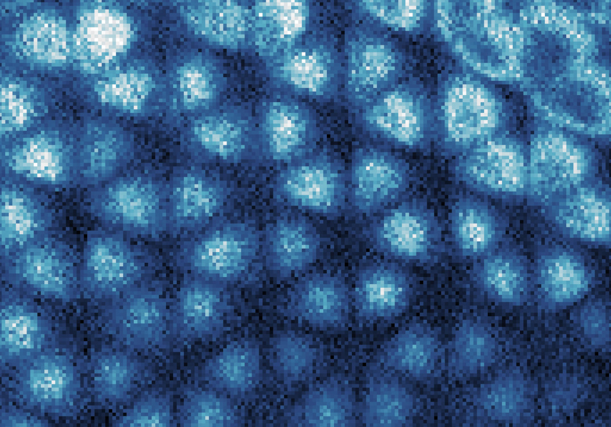
Electrons typically travel at high speeds, zipping through matter unbound. In the 1930s, physicist Eugene Wigner predicted that electrons could be coaxed into stillness at low densities and cold temperatures, forming an electron ice that would later be called the Wigner crystal. Ninety years later, in 2021, a team led by Feng Wang and Michael Crommie, Berkeley Lab senior faculty scientists in the Materials Sciences Division and UC Berkeley physics professors, provided direct evidence that these electron crystals exist.
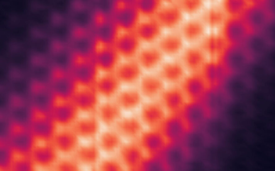
Now Wang, Crommie, and their teams have captured direct images of a new quantum phase of an electron solid – the Wigner molecular crystal. Their findings were reported in the journal Science.
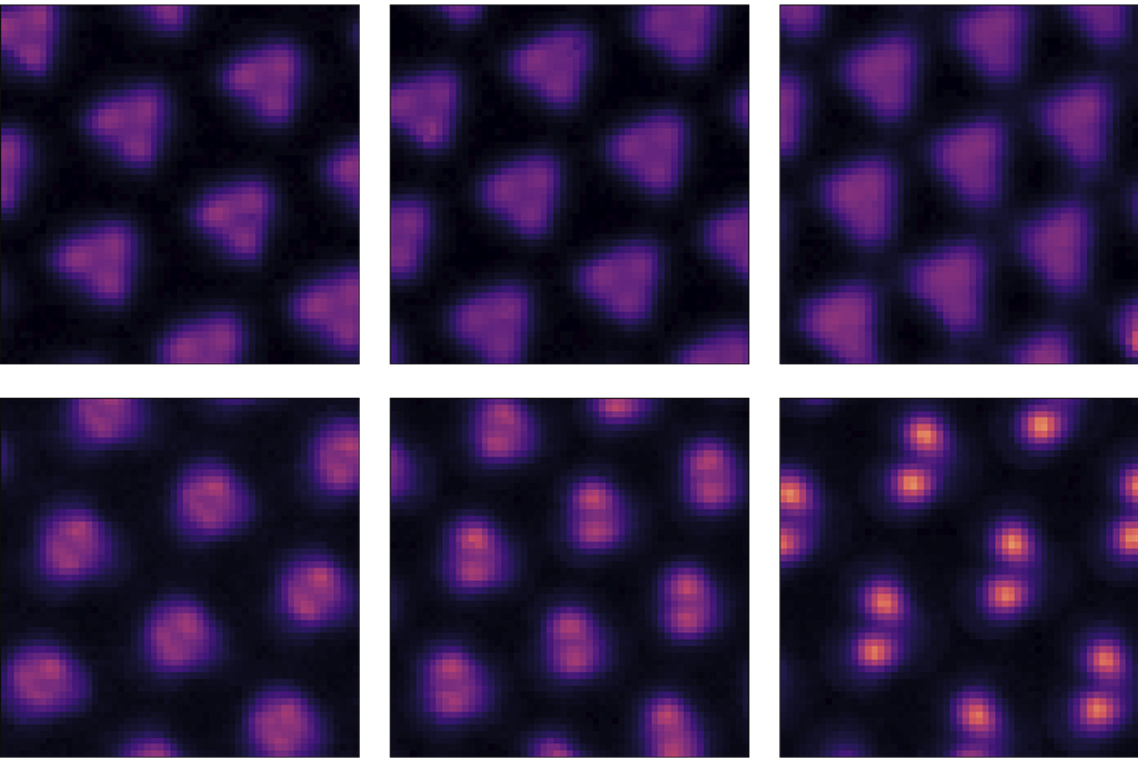
Whereas Wigner crystals or electron ice are characterized by a honeycomb arrangement of electrons, Wigner molecular crystals have a highly ordered pattern of artificial “molecules” made of two or more electrons.
“We are the first to directly observe this new quantum phase, which was quite unexpected,” Wang said. “It’s pretty exciting.”
For many years, scientists have tried to capture direct images of the Wigner molecular crystal, but their progress has been hindered by the tendency of the STM tip to destroy the material’s electron configuration.
In the new study, the Berkeley Lab researchers overcame this hurdle by minimizing the electric field from the STM tip, an advance that allowed them to see the Wigner molecular crystal’s delicate electronic structure.
During experiments at Wang’s lab, they formed a nanomaterial called a “twisted tungsten disulfide (tWS2) moiré superlattice” by placing an atomically thin bilayer of tungsten disulfide (WS2) on top of a 49-nanometer-thick layer of hBN (hexagonal boron nitride) and a graphite back gate. The WS2 layers are stacked on top of each other at a 58-degree twist angle.
Using their STM technique, they found that doping the tWS2 moiré superlattice with electrons filled each 10-nanometer-wide unit cell of the material with just two or three electrons. And in a surprising result, these filled unit cells formed an array of moiré electron molecules throughout the superlattice – resulting in a Wigner molecular crystal.
“Low temperatures along with the energy potential created by the tWS2 moiré superlattice confine the electrons locally,” Wang explained, adding that “the interplay between quantum mechanics and the electron-electron interaction drives the localized electrons into Wigner molecule states.”
In future experiments, Wang, Crommie, and team hope to use their new STM technique to gain a better understanding of this new quantum phase and see what potential applications it could lead to.
This work was supported by the DOE Office of Science. Additional funding was provided by the National Science Foundation.
###
Lawrence Berkeley National Laboratory (Berkeley Lab) is committed to delivering solutions for humankind through research in clean energy, a healthy planet, and discovery science. Founded in 1931 on the belief that the biggest problems are best addressed by teams, Berkeley Lab and its scientists have been recognized with 16 Nobel Prizes. Researchers from around the world rely on the Lab’s world-class scientific facilities for their own pioneering research. Berkeley Lab is a multiprogram national laboratory managed by the University of California for the U.S. Department of Energy’s Office of Science.
DOE’s Office of Science is the single largest supporter of basic research in the physical sciences in the United States, and is working to address some of the most pressing challenges of our time. For more information, please visit energy.gov/science.

Basics 2 Breakthroughs

New Technique Lets Scientists Create Resistance-Free Electron Channels

