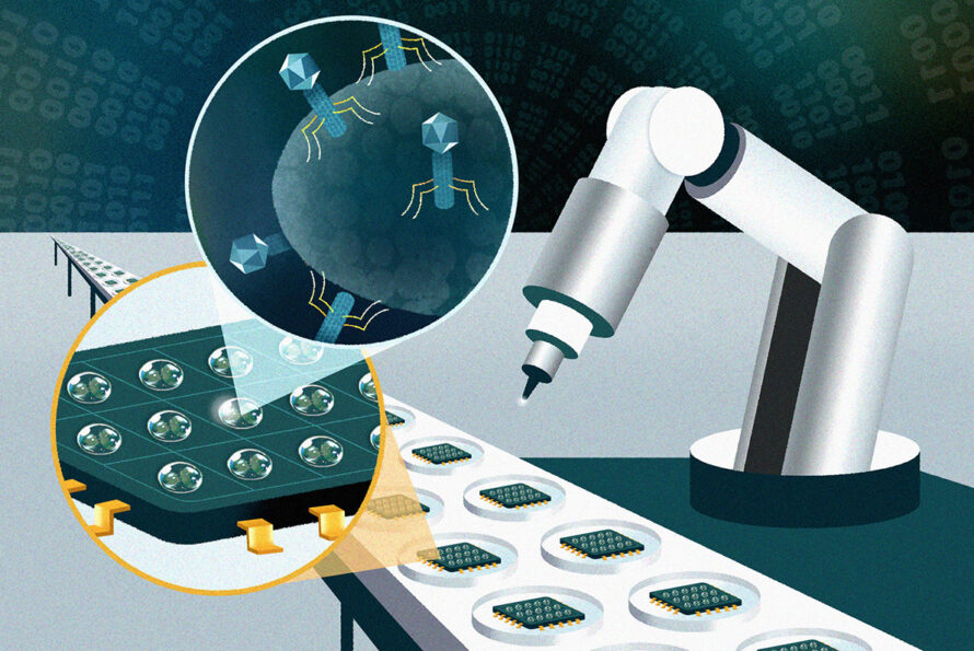
Combatting Antibiotic Resistance with Nanotechnology, Robotics, and AI
What’s the Problem with Quantum Noise?
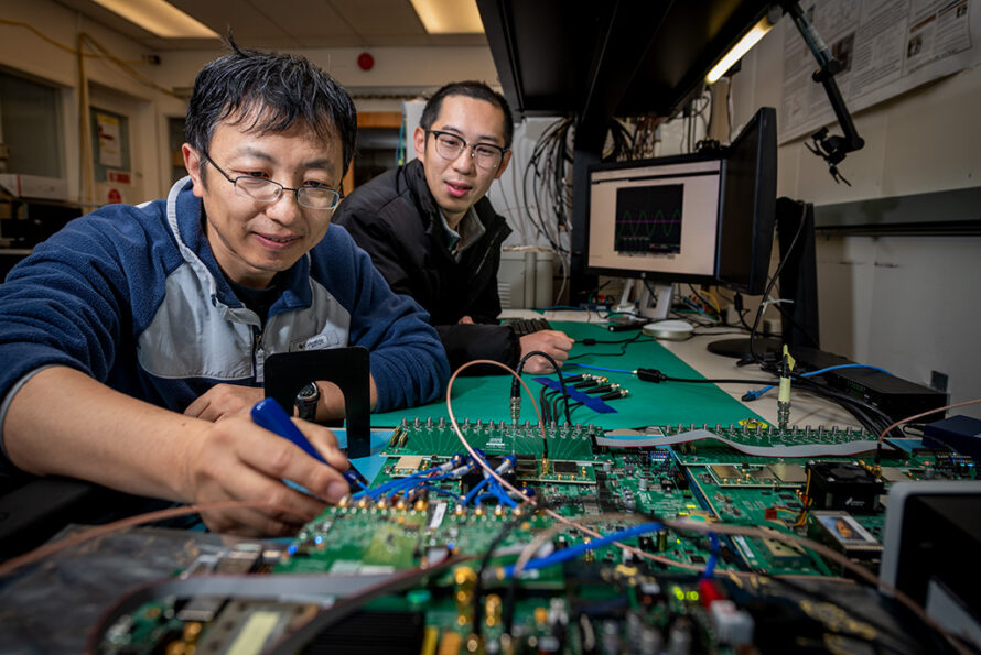
Partnering with Industry to Accelerate Quantum Computing
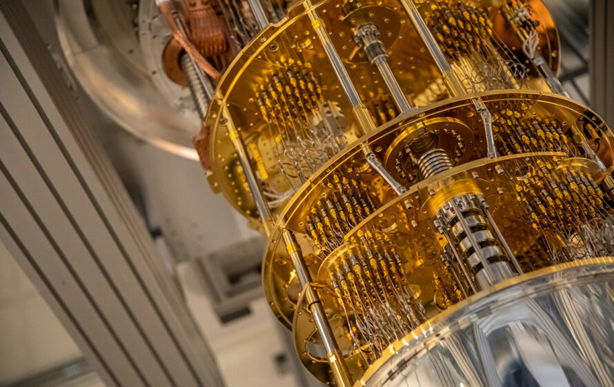
Stacking Up for the Future: How Researchers Are Building Next-Gen Quantum Computers
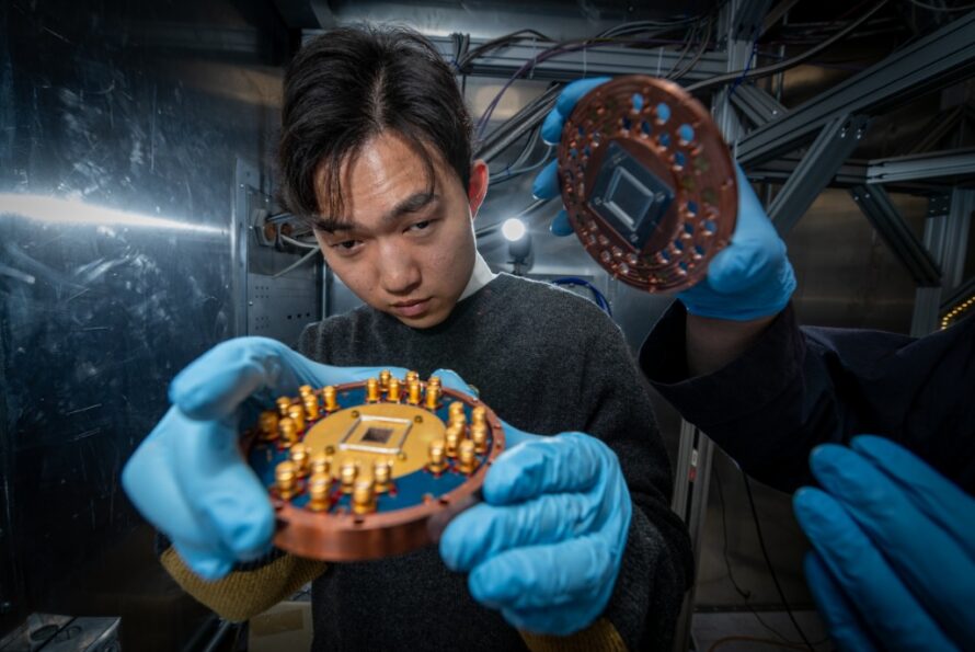
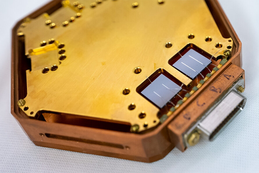
Solving a Mystery in Dark Matter Detectors Could Improve Quantum Computers
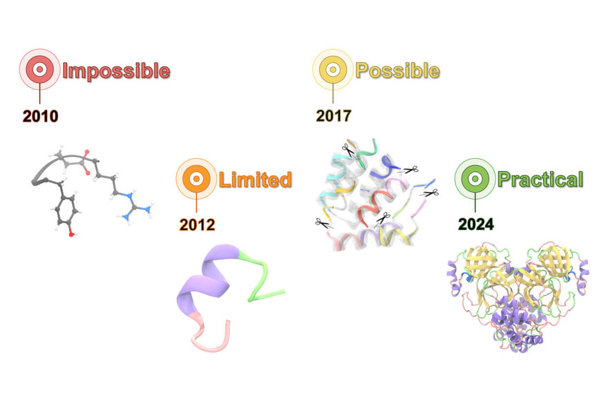
Cracking the Code: Using AI to Solve Difficult-to-Map Proteins
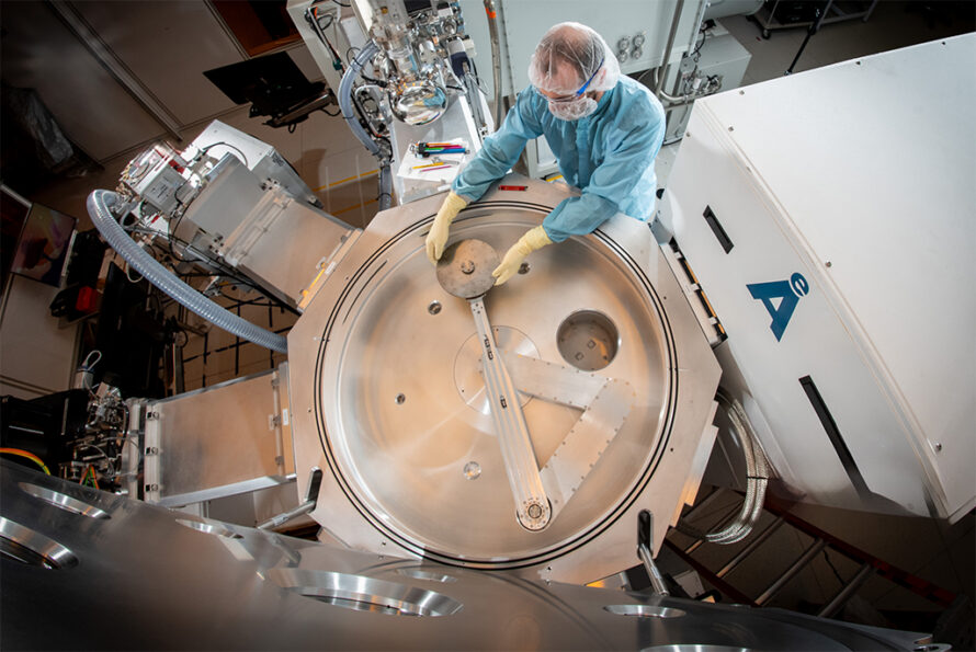
A ‘Robot Pizza Chef’ Serving Up Better Quantum Computers
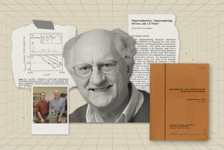
How John Clarke's Nobel Prize-Winning Research Paved the Way for Quantum Computing
Berkeley Lab’s Big Science Stories of 2025
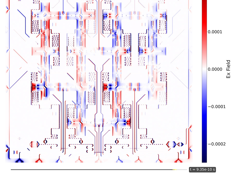
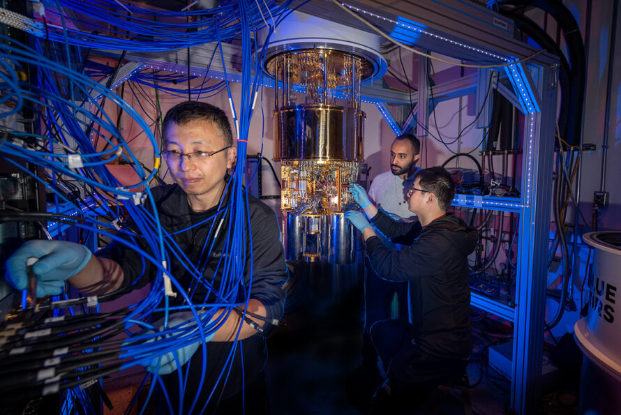
Unprecedented Perlmutter Simulation Details Quantum Chip
The Quantum Systems Accelerator Embarks on Next Five Years of Pioneering Quantum Technologies for Science
New Berkeley Lab and NVIDIA Partnership Integrates Quantum and AI Supercomputing for Next-Generation Research